About Us
A few words about us
The Research & Development activity on photovoltaics,
currently present in the Casaccia Research Center in Rome, was born in the mid-eighties
together with the new role that ENEA assumed in the field of renewable energy sources.
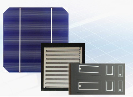
The activity initially focuses on the realization of solar cells in GaAs and crystalline silicon,
as well as on the characterization of modules, components and photovoltaic systems.
Over time, the activities have focused more on crystalline silicon, which in the meantime
has become the most used material in the photovoltaic field. In the last 10 years new technologies
have been added, in particular heterojunctions and multi-junctions with particular attention to new materials.
-
Mission
The research group DTE-FSN-TEF, Department of Energy Technologies - Photovoltaics and Smart Network -
Manufacturing Technologies of photovoltaic cells, is made up of nine researchers, seven technicians,
one secretary, three research grant holders, a doctoral student.
The activities of the laboratory concern the study and implementation of devices
photovoltaics based on conventional materials such as monocrystalline silicon,
polycrystalline and amorphous. Conducts studies and research on the use of new materials
for photovoltaics such as CZTS, CTS and transparent and conductive oxides.
It also develops process technologies and systems for the construction of devices
of new generation such as heterojunctions and multi-junctions with the aid of models
numerical and innovative characterization methods for materials and devices.
Finally he develops photovoltaic systems design with impact assessment on the
network even in the presence of accumulation systems. Develop collaborations, too
international, with universities and industries with attention to the applications of
research activity market.
-
Abilities
- Design and construction of conventional photovoltaic devices such as
silicon homunctions and heterojunctions in amorphous / crystalline silicon with
evaluation of industrial costs
- Research and implementation of innovative materials for photovoltaics
(CZTS, CTS, conductive oxides)
- Design and realization of multi-junction photovoltaic devices and rear contacts
- Design and optimization of processes, conventional and innovative machines
and equipment for the construction of photovoltaic cells at an industrial level
- Realization of numerical models and methods of characterization, also innovative, of
photovoltaic materials and devices
- Development of collaborations with universities, research centers and industry
- Support to the industry of the photovoltaic and manufacturing sector related to it,
in the definition and presentation of projects
- Design and construction of experimental and demonstration photovoltaic systems
- Monitoring of the technological evolution of the market and of the national photovoltaic incentive programs;
identification of research and industrial development opportunities
- Analysis and development of network connection technologies for photovoltaic systems
also in accumulation presents